555 Multivibrator Circuits Tutorial – Astable, Monostable, Bistable
555 Timer IC
IC 555 timer IC is one of the most popular integrated circuit chip used for a variety of applications such as astable, monostable, bistable multivibrators, timer circuits, oscillators, PWM (Pulse Width Modulation), PPM (Pulse Position Modulation), square wave generator or pulse generator, etc. Astable mode, Monostable mode and Bistable mode are the three modes of operation of IC 555.
Its low price, simplicity, ease of use, and stability still make it a favorite one for beginners and hobbyists.
The IC 556 and IC 558 are 14 pins dual timer and 16 pin quad timer versions of the IC 555 respectively. IC 7555 is the CMOS version of the 555 IC with same pin configuration and function.
Internal Diagram of 555 timer IC
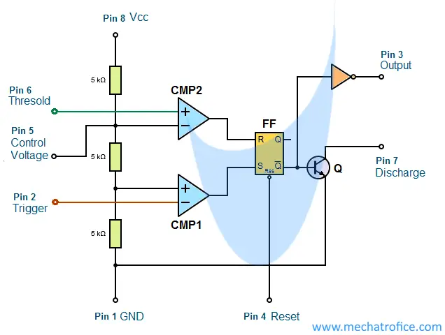
555 internal circuit consists of three series 5K resistors connected between the Vcc and GND. Thus the voltage drop across each resistance in the series network is Vcc/3. Hence, the voltage at the non-inverting input of comparator 1 will be 1/3Vcc and at the inverting input of comparator 2 will be 2/3Vcc of the supply voltage.
The outputs of the comparator 1 and comparator 2 is connected to the R and S input of the SR flip-flop respectively. The Q̄ output of the SR flip-flop is connected to the base of the transistor Q and to the inverting buffer circuit. The buffer circuit inverts the input; output 1 for input 0 and 0 for 1. The output pin 3 of the IC is taken from the output of the buffer circuit.
SR flip-flop Truth table
| S | R | Q | Q̄ | State |
| 0 | 0 | Qn | Q̄n | Previous state |
| 1 | 0 | 1 | 0 | Set |
| 0 | 1 | 0 | 1 | Reset |
| 1 | 1 | ? | ? | Invalid |
When the voltage at pin2 and pin6 is less than 1/3Vcc the output states of the Comp 1 and Comp 2 becomes HIGH and LOW or 1 and 0 respectively. S=1 & R=0, Q̄ =0, the output switches to a HIGH state ( inverse of the Q̄ state).
The outputs of both comparators remain in a LOW state when the voltage at Pin 2 and Pin6 is greater than 1/3Vcc but less than 2/3Vcc. S=0 & R=0, Q̄ =Q̄n, the output remains in the previous state.
When the voltage at Pin2 and Pin6 is greater than 2/3Vcc the Comp 1 and Comp 2 has an output state of 0 and 1 respectively.S=0 & R=1, Q̄ =1, the output switches to a LOW state.
555 timer Pin configuration

By Inductiveload – Own work, Public Domain, Link
Pin1 GND: Ground
Pin2 Trigger: The output switches to the HIGH state, when the voltage at the pin2 becomes less than 1/3 of the supply voltage.
Pin 3 Output: The output pin; either a HIGH state or LOW state output. It can drive a maximum current of 200 mA.
Pin 4 Reset: An active-low input. Resets the IC when the voltage at the pin is below 0.7V (Output switches to LOW). Normally connected to the positive terminal of the supply.
Pin 5 Control Voltage: It is connected directly to the voltage divider; across two series resistors at 2/3Vcc. Hence, the threshold value will be always equal to the voltage at pin 5 (2/3Vcc) and the trigger input (1/3Vcc) will have half of its value.
So, by adjusting the voltage at the control pin the threshold and triggering voltages can be overridden. Pulse width modulation, Pulse position modulation, etc. with the 555 IC are done by using this function of the IC.
Normally, when the control pin is not used a bypass capacitor of value 10nF will be connected across the control pin and ground for eliminating any voltage fluctuations and noises.
Pin 6 Threshold: When the voltage at the pin 6 comes above 2/3 of the supply voltage, the output switches to a LOW state.
Pin 7 Discharge: Pin for the discharge of the capacitor. It is connected to the open collector of the internal transistor. The emitter of the transistor is grounded and the base input is a complement of the IC output. So when the output is a LOW state, Pin7 becomes grounded.
Pin 8 +Ve Supply: Power supply input with a voltage range 4.5V to 15V.
Specifications of 555 IC
Operating Voltage: 4.5 to 16V
Max Output current: ± 200 mA; sink or source
Reset Voltage: 0.4 to 1V
Packages: DIP-8 and SIP-8
555 Timer Astable multivibrator
An astable multivibrator output consists of two quasi-stable states, that is it has no stable states in either HIGH or LOW states.
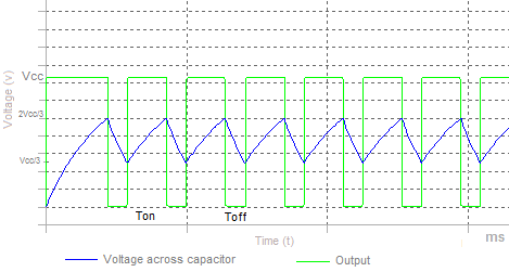
The output remains in either High state or Low state for a time T1 and then changes to the opposite state for a time T2. And the cycle repeats. The time period of a complete square wave, T = T1 + T2.
The frequency of oscillation f = 1/ T
Duty cycle is the ratio of ON time (duration of HIGH state or pulse width) to the total time period of a cycle. The duty cycle of an Astable multivibrator = TON/ TON + TOFF
Working of astable multivibrator Circuit
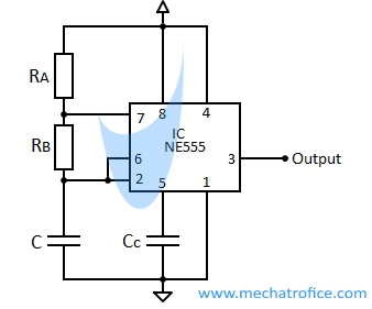
Initially, the voltage across the trigger and threshold input is below 1/3Vcc. Hence, the output switches to the high state and remains the state until the threshold input reaches 2/3Vcc. Gradually the capacitor C starts charging towards the supply voltage Vcc through resistor RA and RB. When the voltage across the capacitor charges to 2/3 Vcc, the output switches to the low state and the capacitor starts to discharge through resistor RB. The output state remains in the low state until the voltage across the capacitor discharges to 1/3Vcc. When the voltage reaches to 1/3Vcc the capacitor stops discharging and again the charging begins. The cycle repeats which generates a periodic square wave.
Formula derivation of 555 astable multivibrator
The ON time and OFF time of the astable multivibrator circuit can be calculated by taking the charging and discharging time of the capacitor C. The ON time of a cycle is equal to the charging time of the capacitor from 1/3Vcc to 2/3Vcc and the OFF is equal to the discharge time from 2/3Vcc to 1/3Vcc.
V(t) is the voltage value across the capacitor at a particular instant of time t.
V(t) = VFinal – (VFinal – VInitial) e -t/RC
During charging, the capacitor is charging towards the source voltage Vcc which is the final voltage. And the initial voltage is 1/3Vcc which has across the capacitor during the beginning of each cycle.
2Vcc/3 = Vcc – (Vcc -Vcc/3) e -T1/(RA+RB) C
T1 is the time required to charge the capacitor C through resistance RA + RB from the voltage 1/3Vcc to 2/3Vcc by the source Vcc.
2Vcc/3 = Vcc – 2Vcc/3 e -T1/(RA+RB) C
Vcc – 2Vcc/3 = 2Vcc/3 e -T1/(RA+RB) C
Vcc/3 = 2Vcc/3 e -T1/(RA+RB) C
1/2 = e -T1/(RA+RB) C
Applying natural log function at both sides of the equation.
In (1/2) =In (e -T1/(RA+RB) C)
-In (2) = -T1/(RA+RB) C | In (1/x) = – In (x)
T1 = In (2) (RA+RB) C | In(2) = 0.69314
Equation for calculating ON time, T1 = 0.69 * (RA + RB) * C
Similarly, for the OFF calculate the time period for discharge of capacitor from the voltage 2Vcc/3 to Vcc/3.
Vcc/3 = 2Vcc/3 e –T2/RB * C)
T2 is the time required to discharge the capacitor C through resistance RB.
T2/RB * C = In (2)
Formula for calculating OFF time, T2 = 0.69 * RB * C
The total time period, T = T1 + T2 = TON + TOFF
T = 0.69 * (RA + RB) * C + 0.69 * RB * C
T = 0.69 * (RA + 2RB) * C
555 timer formula for frequency of oscillation, f = 1/ 0.69 * (RA + 2RB) * C
f = 1.44/(RA + 2RB) * C
Duty cycle = T1/ T1 + T2
From the above formula of T1 and T2, the duty cycle can be calculated as, D = (RA+RB)/(RA+2RB)
% Duty cycle, D = (RA+RB)/(RA+2RB) * 100
Astable multivibrator using 555 timer with diode
The above 555 astable mutivibrator circuit can only generate an output which has a duty cycle above 50%. Because as the charging resistance is RA+RB and discharging resistance is RB, the T1 or the ON period will be always greater than the OFF period. Thus a duty cycle below 50% is not possible with the normal 555 astable circuit.
So in order to charge and discharge the capacitor through different resistors, a bypass diode is added in the below circuit. Hence, during charging the Diode D bypass the resistance RB and the charging current flows through RA and D. And the discharge as same as normal circuit through the RB.
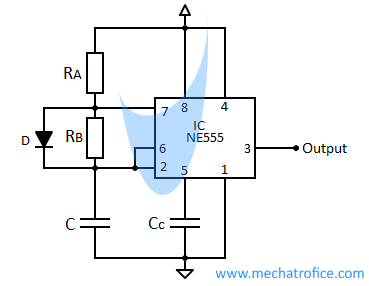
Astable multivibrator with diode formula derivation
Here the charging and discharging is done through two independent resistors the formula derivation is same as the above 555 astable multivibrator circuit except for the charging resistor.
ON time Formula, T1 = 0.69 * RA * C
OFF time Formula, T2 = 0.69 * RB * C
The total time period, T = T1 + T2 = TON + TOFF
T = 0.69 * RA * C + 0.69 * RB * C
T = 0.69 * (RA + RB) * C
Here we get a Duty cycle, D = RA/(RA+RB)
Duty cycle in %, D = RA/(RA+RB) * 100
555 Monostable Multivibrator
Monostable multivibrator has only one stable state. The output of the circuit switches to a quasi stable state on receiving the trigger pulse and after a time period T the output return to its stable state. It remains the stable state until next trigger signal is received.
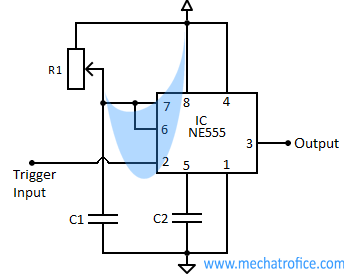
In a monostable multivibrator, an external trigger pulse is required for the transition of output from the stable state to quasi-stable state.
During the LOW state of the output, the capacitor remains fully discharged and the supply voltage drops across the resistance R1 through the discharge pin 7.
When an external negative pulse is applied to the Pin 2 trigger input, it switches the output HIGH and the capacitor C1 starts charging towards the supply voltage Vcc through resistance R1. Once the capacitor reaches the voltage 2/3Vcc the Output switches to a LOW or stable state and the capacitor discharges instantly. The state remains till next pulse is applied.
555 Monostable multivibrator formula derivation
The time period of the quasi-stable state or ON time is the charging time of the capacitor C from 0 to 2/3Vcc through resistance R1 by the source votlage Vcc.
2Vcc/3 = Vcc (1- e -T/ (R1 * C))
2/3 = 1 – e -T/ (R1 * C))
1/3 = e -T/ (R1 * C))
Applying natural logarithm,
In (1/3) =In (e -T/ (R1 * C))
-In (3) = -T/(R1* C ) | In (1/x) = – In (x)
T = In (3) (R1 *C )
Equation for calculating ON time, T1 = 1.1 * R * C
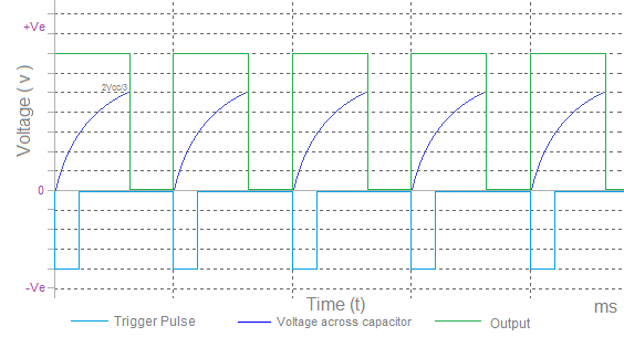
Bistable Multivibrator using 555 timer
A bistable multivibrator has two stable states. The circuit remains in any one of the two stable states unless external trigger pulse is applied.
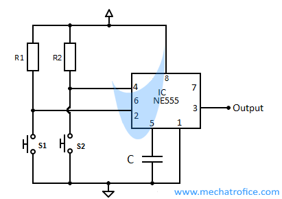
Here the trigger and reset input is connected across the switch s1 and switch s2 respectively. One terminal of both switches are connected to the positive of the supply through a resistor (around 10k) and the other terminal to ground.
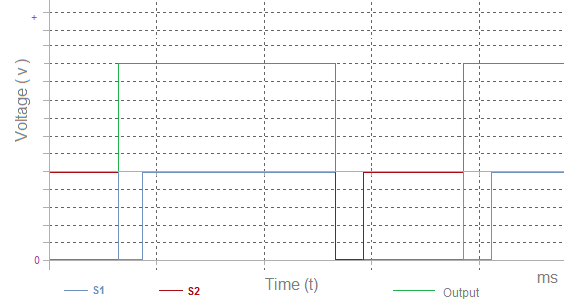
When the switch S1 is pressed the trigger input is grounded (voltage at trigger input gets below Vcc/3) and the Output switches to a HIGH state. And when S2 has pressed the IC resets which switches the output to LOW. It is represented in the above timing diagram, how the output changes with the input during the switch press of s1 & s2.
See more 555 IC Projects