Zener diode voltage regulator circuits
The Zener Diode Voltage Regulator is a simple, cost-effective device used in many electronic circuits to provide a desired level of stable voltage. This is achieved by the Zener diode’s unique property of maintaining a constant voltage across itself when the current passing through it reverses after reaching its breakdown voltage.
Basic voltage regulator circuit
How a zener diode works as a voltage regulator can be easily understood by analyzing the circuit below. As the zener diode is connected in a reverse bias configuration parallel to the load. When the input voltage exceeds the Zener voltage (Vz), the diode enters the breakdown region and allows current to flow, maintaining a constant voltage across the load.
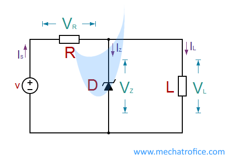
The voltage difference between the input voltage VS and VZ will be dropped across the resistance R. The circuit arrangement and calculation are the same as the above reference circuit, but here discuss the circuit to provides a regulated supply to a load with a particular power rating.
VR = VS – VZ
(IZ + IL) * R = VS – VZ.
A minimum zener current of around 10mA needs to be maintained to keep its regulated voltage. The resistor value should be calculated based on the known input voltage and output current value. So it can provide the minimum Zener current under full load condition. Because when the full load has applied the voltage across the Zener should not be dropped below Vz. Vs- Vr should be always equal to the rated value of the zener. As the drop across the R increases with load current, vs- VR should not come lower than Vz. In such conditions the output voltage decreases than the required regulated value.
Also while selecting the R the power dissipation capacity for the Zener diode should be considered. The Iz should not exceeds the value greater than the maximum permitted current through the zener, which is based on its power rating.
Zener voltage regulator calculation
- Design a zener voltage regulator circuit to drive a load of 6V, 100mW from an unregulated Input supply of Vmin = 8V, Vmax = 12V using a 6V zener diode?
VS – VZ = VR; 8V – 6V = 2V.
Let take a minimum current Iz as 10mA at Full Load.
IL = 0.10/6 = 16mA
Resistor calculation for the above zener voltage regulator circuit,
(IZ + IL) * R = VS – VZ; (10mA + 16mA) * R = 2V
R = 2/93mA = 21Ω
The voltage across the zener remains a constant value VZ for any increase in the input voltages above VZ. The zener and Load resistance is in parallel. Hence the VZ = VL; the voltage across the load will always remain a constant 6V.
Power Dissipation: The power dissipation of a Zener diode is an important factor to consider during design, as it indicates the amount of power the diode can dissipate as heat without damaging itself.
Limitations: While Zener diodes are excellent for small changes in input voltage and load resistance, they are not suitable for large changes due to their limited power dissipation capacity.
Zener diode transistor series voltage regulator
A transistor Series Voltage Regulator is basically an emitter follower configuration with a fixed base voltage. The load is connected in series to the transistor, i.e. the load current is connected to the emitter of the transistor. Hence the Load current IL is equal to the base current IE (IE = IL).
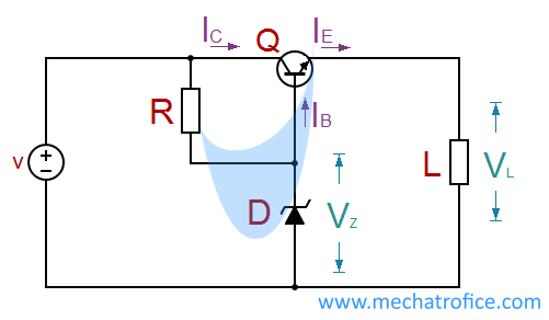
The base voltage is equal to zener voltage VZ, which always remains as a constant for any applied input voltage above value VZ.
IB + IC = IE = IL | IB – Base current.
IL = VOUT / R = (VZ – VBE)/R = P / VOUT. P – Load power rating.
IL = IB β + IB; IB = IL / (1+ β) | β – Amplification factor or hfe.
VS-VZ = (IB + IZ) R
Resistance, R = VS – VZ / (IB + IZ)
VBE – Base-emitter junction voltage around 0.6 to 0.7V.
VOUT= VZ – VBE
Hence a regulated constant output voltage can be obtained at the output from an unregulated supply.
- Design for a Zener Transistor series voltage regulator circuit to drive a load of 6V, 1w, from a supply of 10V with a ±3V ripple voltage
From the above formula,
IL = 1 / 6 = 167mA
By assuming the value of β as 220 the calculated IB value is 759µA; calculate IB based on the hfe or β value of the transistor using in the circuit.
Assume a minimum IZ of 10mA. Then the R = 7/ (10mA + 759µA) = 650Ω
Let’s take a zener diode of 6.8V, then the output voltage, VOUT = VZ – VBE
6.8V – 0.7 = 6.1V
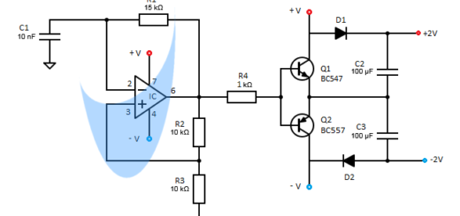
Zener diode voltage regulator circuit using op-amp
The op-amp voltage regulator circuit consists of a non-inverting amplifier with a fixed reference voltage at the non-inverting input. The negative feedback taken from the output is connected to the inverting pin of the op-amp through a voltage divider.
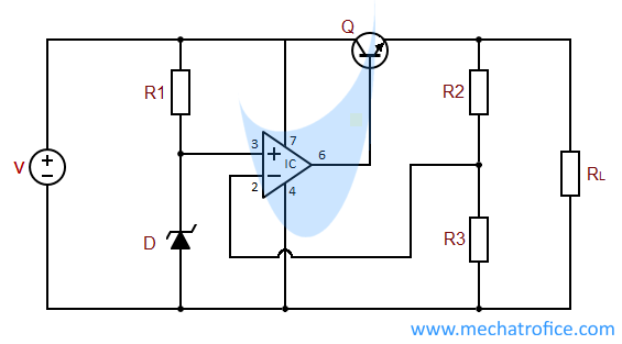
As similar to a non-inverting op-amp circuit the output generates a voltage value so as to obtain an equal voltage of non-inverting pin at the inverting input. Hence the circuit output voltage adjusts itself so as to obtain a voltage across the R3 equal to value Vz. Unlike other above circuits, the op-amp voltage regulator has a constant zener current which doesn’t vary with the input voltage changes or load changes.
Here circuit the zener just provides the reference voltage to the op-amp. As the op-amp IC has a high input impedance, the current through R1 will be almost equal to the zener current Iz.
VOUT = VZ * (R2+R3) / R3
= VZ * (1+ R2/R3)
By varying the resistance of R2 and R3 we can adjust the output voltage of the circuit to the required voltage values. Also, a potentiometer can replace resistance R3 to make it a variable power supply. This circuit can obtain output voltage values higher than the zener value VZ by using the zener voltage as a reference value.
6V op-amp voltage regulator
- Design for an op-amp voltage regulator circuit to drive a load of 6V,1.2W from an Input supply of 12V with a ±2V ripple voltage, using a 3V zener diode.
Refer to the voltage reference circuit to set the resistance R1. Let’s take the value of R2 as 1kΩ.
Using the formula given above for VOUT, the R3 calculated as 1kΩ for a 6V output with a 3V zener diode.
Components Required
IC – 741
Resistor – R1 – 150, R2,R3 – 1k
Diode – D – 3V
Transistor – Q – 2N222
AC to DC
- Rectifier circuit
- Filter circuit
- Voltage regulator circuit