Voltage Doubler Circuit schematic using 555, op amp & AC to DC
AC to DC Voltage Doubler Circuit
A voltage doubler is a circuit that produces an output voltage that is double the applied input voltage. The below diagram is an AC to DC voltage doubler circuit. That is the input supply is an AC source that is converted to a DC output with a voltage value of two times the input AC voltage.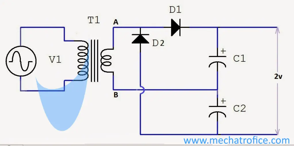 In this circuit, the capacitors C1 and C2 charge alternately in the two half cycles of the AC source. So, the total voltage across the two capacitors becomes equal to the sum of the voltage of two capacitors.
On the positive half cycle, the diode D1 is forward biased and D2 is reverse biased, thus the current drive through the path from A to B via Diode D1 and capacitor C1. Now the capacitor C1 charges and the voltage across the capacitor C1 becomes equal to the voltage across AB.
On the negative half cycle, the D2 forward biased and D1 reverse biased, thus the current flows from B to A through capacitor C2 and D2. Hence the voltage across C2 also becomes equal to the VAB.
So, the total voltage taken across the C1 and C2 becomes V=VAB+VAB=2VAB.
To maintain the output voltage as twice as its input, use a load with high resistance or use a larger capacitance. So the capacitor can be charged in each cycle before it discharges to a lower voltage level.
Voltage doubler circuit using 555
Here the circuit is a voltage doubler or DC to DC converter using a 555 IC. The circuit consists of an astable multivibrator circuit that generates a square wave at the output terminal 3, with a 50% duty cycle. The capacitors C1 and C2 charge alternately with the ON and OFF state of the output. When the output is low the capacitor C1 charges and at the high state capacitor C2 charges. Diode D2 and D3 prevent the discharging of the capacitors.
 The applied input voltage should be at the limit of IC NE555 operating voltage 4.5 V- 16V. If the input voltage is V (4.5 V- 16 V) then the output voltage taken across the capacitors will be 2V, which is double the supply voltage. The output values may have slight variations; they should measure properly before applying to any components or device. Also, the output load should have minimum resistance to prevent over-discharge of the capacitor.
Components required
IC – NE555
Resistor – R1, R2 – 39K
Capacitor – C1, C2 – 100uf, C3, C4 – 10nf
Diode – D1, D2, D3 -1N4007
Supply – 4.5V -16V
Simple DC Voltage doubler circuit diagram using op-amp
This voltage doubler circuit also consists of an astable multivibrator, using an Op-amp IC 741. Similar to a 555 voltage doubler, the here circuit also generates a square wave output of a specific time period which switches the output states HIGH and LOW. The base of both NPN and PNP transistors, BC547 and BC557 respectively are connected to the op-amp output.
So, during the high state of the op-amp o/p, the transistor Q1 will be active and the capacitor C3 gets charged. And in the low state, the transistor Q2 will be active and capacitor C2 charges. Therefore the total potential across both capacitors will be double the supply voltage. Because the value equal to the supply voltage is stored in each capacitor alternatively during each high and low state of the o/p.
The capacitor C1 and Resistor R3 should connect to the ground or zero voltage point of the supply.
Components required
IC- 741
Resistor – R1 – 15k, R2, R3 – 10k, R4 – 1k
Capacitor – C1 – .01uf, C2, C3 – 100uf
Transistor – Q1 – BC547, Q2 – BC557
Diode – D1, D2 – 1N4007
Which way do the 100uF caps go in the 555 circuit? And, should there be connection dots on both sides of both of those resistors?
This is the 3rd 555 voltage doubler circuit I’ve tried to build today. I can’t get any of them to work.
The positive terminal of the electrolytic capacitor to positive of output or cathode of D1 and negative terminal to -ve of output or Anode of D2.
Yes, both sides of resistors have a connection.